This section describes the connectors on the Emerald-MM-8Plus board.
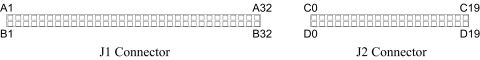
Connectors J1 and J2 carry the ISA bus signal. Figure 1 shows the PC/104 A and B pin layout for J1, and the C and D pin layout for J2. These signals are not used to communicate with the CPU but are pass to other cards on the PC/104 stack.
| J1 Connector Pinout | J2 Connector Pinout | ||||||
| IOCHCHK- | A1 | B1 | GND | GND | C0 | D0 | GND |
| SD7 | A2 | B2 | RESETDRV | SBHE- | C1 | D1 | MEMCS16-- |
| SD6 | A3 | B3 | +5V | LA23 | C2 | D2 | IOCS16- |
| SD5 | A4 | B4 | IRQ9 | LA22 | C3 | D3 | IRQ10 |
| SD4 | A5 | B5 | -5V | LA21 | C4 | D4 | IRQ11 |
| SD3 | A6 | B6 | DRQ2 | LA20 | C5 | D5 | IRQ12 |
| SD2 | A7 | B7 | -12V | LA19 | C6 | D6 | IRQ15 |
| SD1 | A8 | B8 | ENDXFR- | LA18 | C7 | D7 | IRQ14 |
| SD0 | A9 | B9 | +12V | LA17 | C8 | D8 | DACK0- |
| IOCHRDY | A10 | B10 | keyed | MEMR- | C9 | D9 | DRQ0 |
| AEN | A11 | B11 | SMEMW- | MEMW- | C10 | D10 | DACK5- |
| SA19 | A12 | B12 | SMEMR- | SD8 | C11 | D11 | DRQ5 |
| SA18 | A13 | B13 | IOW- | SD9 | C12 | D12 | DACK6- |
| SA17 | A14 | B14 | IOR- | SD10 | C13 | D13 | DRQ6 |
| SA16 | A15 | B15 | DACK3- | SD11 | C14 | D14 | DACK7- |
| SA15 | A16 | B16 | DRQ3 | SD12 | C15 | D15 | DRQ7 |
| SA14 | A17 | B17 | DACK1- | SD13 | C16 | D16 | +5 |
| SA13 | A18 | B18 | DRQ1 | SD14 | C17 | D17 | MASTER- |
| SA12 | A19 | B19 | REFRESH- | SD15 | C18 | D18 | GND |
| SA11 | A20 | B20 | SYSCLK | keyed | C19 | D19 | GND |
| SA10 | A21 | B21 | IRQ7 | ||||
| SA9 | A22 | B22 | IRQ6 | ||||
| SA8 | A23 | B23 | IRQ5 | ||||
| SA7 | A24 | B24 | IRQ4 | ||||
| SA6 | A25 | B25 | IRQ3 | ||||
| SA5 | A26 | B26 | DACK2- | ||||
| SA4 | A27 | B27 | TC | ||||
| SA3 | A28 | B28 | BALE | ||||
| SA2 | A29 | B29 | +5V | ||||
| SA1 | A30 | B30 | OSC | ||||
| SA0 | A31 | B31 | GND | ||||
| GND | A32 | B32 | GND | ||||
The PC/104-Plus bus is essentially identical to the PCI Bus except for the physical design. A single pin and socket connector is specified for the bus signals. A 120-pin header, J3, arranged as four 30-pin rows incorporates a full 32-bit, 33MHz PCI Bus. The additional pins on the PC/104-Plus connectors are used as ground or key pins. The female sockets on the top of the board enable stacking another PC/104-Plus board on top of the Emerald-MM-8Plus board. The Emerald-MM-8Plus board should be the bottom board of a PC/104-Plus stackup.
In the connector J3 pinout table, below, the top corresponds to the left edge of the connector when the board is viewed from the primary side (the side with the female end of the PC/104-Plus connector), and the board is oriented so that the PC/104 connectors are along the bottom edge of the board and the PC/104-Plus connector is in the top of the Emerald-MM-8Plus board.
| 1 | GND/5.0V KEY | Reserved | +5V | AD00 |
| 2 | VI/O | AD02 | AD01 | +5V |
| 3 | AD05 | GND | AD04 | AD03 |
| 4 | C/BE0* | AD07 | GND | AD06 |
| 5 | GND | AD09 | AD08 | GND |
| 6 | AD11 | VI/O | AD10 | M66EN |
| 7 | AD14 | AD13 | GND | AD12 |
| 8 | +3.3V | C/BE1* | AD15 | +3.3V |
| 9 | SERR* | GND | Reserved | PAR |
| 10 | GND | PERR* | +3.3V | Reserved |
| 11 | STOP* | +3.3V | LOCK* | GND |
| 12 | +3.3V | TRDY* | GND | DESEL* |
| 13 | FRAME* | GND | IRDY* | +3.3V |
| 14 | GND | AD16 | +3.3V | C/BE2* |
| 15 | AD18 | +3.3V | AD17 | GND |
| 16 | AD21 | AD20 | GND | AD19 |
| 17 | +3.3V | AD23 | AD22 | +3.3V |
| 18 | IDSEL0 | GND | IDSEL1 | IDSEL2 |
| 19 | AD24 | C/BE3* | VI/O | IDSEL3 |
| 20 | GND | AD26 | AD25 | GND |
| 21 | AD29 | +5V | AD28 | AD27 |
| 22 | +5V | AD30 | GND | AD31 |
| 23 | REQ0* | GND | REQ1* | VI/O |
| 24 | GND | REQ2* | +5V | GNT0* |
| 25 | GNT1* | VI/O | GNT2* | GND |
| 26 | +5V | CLK0 | GND | CLK1 |
| 27 | CLK2 | +5V | CLK3 | GND |
| 28 | GND | INTD* | +5V | RST* |
| 29 | +12V | INTA* | INTB* | INTC* |
| 30 | -12V | ~REQ3 | ~GNT3 | GND/3.3V KEY |
On the Emerald-MM-8Plus, the octal UART is connected to the PCI bus and is powered by 5V with its PCI interface powered by the PCI bus VIO, which can be 3.3V or 5V. For this reason, the connector is not keyed (to prevent certain types of cards from being inserted).
Emerald-MM-8Plus provides two identical 40-pin headers labeled J4 and J5 for the serial ports. Four ports are contained on each header.
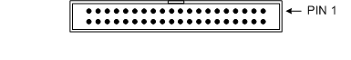
Connector, J4,is for ports 1-4 and is located along the right side of the board.
| J4 Port No. | Pin Assignment |
| PORT1 | Pins 1 - 10 |
| PORT2 | Pins 11 - 20 |
| PORT3 | Pins 21 - 30 |
| PORT4 | Pins 31 - 40 |
Connector, J5, is for ports 5-8 and is located along the left side of the board.
| J5 Port No. | Pin Assignment |
| PORT5 | Pins 1 - 10 |
| PORT6 | Pins 11 - 20 |
| PORT7 | Pins 21 - 30 |
| PORT8 | Pins 31 - 40 |
Pin numbers are marked on the board to assist with connector orientation.
Diamond Systems Corporation Cable Assembly Number C-DB9M-4 connects this header to four DE-9 Male connectors, for direct connection to RS-232-C signaling. The following tables list the signals for the appropriate mode of operation, as well as the DE-9 pin numbers to which these signals are wired.
| J5 | - | J4 | ||||||
| Port1: DCD1 | 1 | 2 | DSR1 | Port5: DCD5 | 1 | 2 | DSR5 | |
| RXD1 | 3 | 4 | RTS1 | RXD5 | 3 | 4 | RTS5 | |
| TXD1 | 5 | 6 | CTS1 | TXD5 | 5 | 6 | CTS5 | |
| DTR1 | 7 | 8 | RI1 | DTR5 | 7 | 8 | RI5 | |
| GND | 9 | 10 | DIO0 | GND | 9 | 10 | DIO4 | |
| Port2: DCD2 | 11 | 12 | DSR2 | Port6: DCD6 | 11 | 12 | DSR6 | |
| RXD2 | 13 | 14 | RTS2 | RXD6 | 13 | 14 | RTS6 | |
| TXD2 | 15 | 16 | CTS2 | TXD6 | 15 | 16 | CTS6 | |
| DTR2 | 17 | 18 | RI2 | DTR6 | 17 | 18 | RI6 | |
| GND | 19 | 20 | DIO1 | GND | 19 | 20 | DIO5 | |
| Port3: DCD3 | 21 | 22 | DSR3 | Port7: DCD7 | 21 | 22 | DSR7 | |
| RXD3 | 23 | 24 | RTS3 | RXD7 | 23 | 24 | RTS7 | |
| TXD3 | 25 | 26 | CTS3 | TXD7 | 25 | 26 | CTS7 | |
| DTR3 | 27 | 28 | RI3 | DTR7 | 27 | 28 | RI7 | |
| GND | 29 | 30 | DIO2 | GND | 29 | 30 | DIO6 | |
| Port4: DCD4 | 31 | 32 | DSR4 | Port8: DCD8 | 31 | 32 | DSR8 | |
| RXD4 | 33 | 34 | RTS4 | RXD8 | 33 | 34 | RTS8 | |
| TXD4 | 35 | 36 | CTS4 | TXD8 | 35 | 36 | CTS8 | |
| DTR4 | 37 | 38 | RI4 | DTR8 | 37 | 38 | RI8 | |
| GND | 39 | 40 | DIO3 | GND | 39 | 40 | DIO7 | |
| Signal | Definition | DE-9 Pin | Direction |
| DCDn | Data Carrier Detect | pin 1 | Input |
| DSRn | Data Set Ready | pin 6 | Input |
| RXDn | Receive Data | pin 2 | Input |
| RTSn | Request to Send | pin 7 | Output |
| TXDn | Transmit Data | pin 3 | Output |
| CTSn | Clear to Send | pin 8 | Input |
| DTRn | Data Terminal Ready | pin 4 | Output |
| RIn | Ring Indicator | pin 9 | Input |
| GND | Ground | pin 5 | Signal Ground |
| DIOn | Digital I/O | - | - |
| J5 | - | J4 | ||||||
| Port1: NC | 1 | 2 | NC | Port5: NC | 1 | 2 | NC | |
| TXD/RXD+1 | 3 | 4 | TXD/RXD-1 | TXD/RXD+5 | 3 | 4 | TXD/RXD-5 | |
| NC | 5 | 6 | NC | NC | 5 | 6 | NC | |
| NC | 7 | 8 | NC | NC | 7 | 8 | NC | |
| GND | 9 | 10 | DIO0 | GND | 9 | 10 | DIO4 | |
| Port2: NC | 11 | 12 | NC | Port6: NC | 11 | 12 | NC | |
| TXD/RXD+2 | 13 | 14 | TXD/RXD-2 | TXD/RXD+6 | 13 | 14 | TXD/RXD-6 | |
| NC | 15 | 16 | NC | NC | 15 | 16 | NC | |
| NC | 17 | 18 | NC | NC | 17 | 18 | NC | |
| GND | 19 | 20 | DIO1 | GND | 19 | 20 | DIO5 | |
| Port3: NC | 21 | 22 | NC | Port7: NC | 21 | 22 | NC | |
| TXD/RXD+3 | 23 | 24 | TXD/RXD-3 | TXD/RXD+7 | 23 | 24 | TXD/RXD-7 | |
| NC | 25 | 26 | NC | NC | 25 | 26 | NC | |
| NC | 27 | 28 | NC | NC | 27 | 28 | NC | |
| GND | 29 | 30 | DIO2 | GND | 29 | 30 | DIO6 | |
| Port4: NC | 31 | 32 | NC | Port8: NC | 31 | 32 | NC | |
| TXD/RXD+4 | 33 | 34 | TXD/RXD-4 | TXD/RXD+8 | 33 | 34 | TXD/RXD-8 | |
| NC | 35 | 36 | NC | NC | 35 | 36 | NC | |
| NC | 37 | 38 | NC | NC | 37 | 38 | NC | |
| GND | 39 | 40 | DIO3 | GND | 39 | 40 | DIO7 | |
| Signal | Definition | DE-9 Pin | Direction |
| TXD/RXD+n | Differential Transceiver Data (HIGH) | pin 2 | bi-directional |
| TXD/RXD-n | Differential Transceiver Data (LOW) | pin 7 | bi-directional |
| GND | Ground | pin 5 | Signal Ground |
| NC | (not connected) | - | - |
| DIOn | Digital I/O | - | - |
| J5 | - | J4 | ||||||
| Port1: NC | 1 | 2 | NC | Port5: NC | 1 | 2 | NC | |
| TXD+1 | 3 | 4 | TXD-1 | TXD+5 | 3 | 4 | TXD-5 | |
| NC | 5 | 6 | RXD-1 | NC | 5 | 6 | RXD-5 | |
| RXD+1 | 7 | 8 | NC | RXD+5 | 7 | 8 | NC | |
| GND | 9 | 10 | DIO0 | GND | 9 | 10 | DIO4 | |
| Port2: NC | 11 | 12 | NC | Port6: NC | 11 | 12 | NC | |
| TXD+2 | 13 | 14 | TXD-2 | TXD+6 | 13 | 14 | TXD-6 | |
| NC | 15 | 16 | RXD-2 | NC | 15 | 16 | RXD-6 | |
| RXD+2 | 17 | 18 | NC | RXD+6 | 17 | 18 | NC | |
| GND | 19 | 20 | DIO1 | GND | 19 | 20 | DIO5 | |
| Port3: NC | 21 | 22 | NC | Port7: NC | 21 | 22 | NC | |
| TXD+3 | 23 | 24 | TXD-3 | TXD+7 | 23 | 24 | TXD-7 | |
| NC | 25 | 26 | RXD-3 | NC | 25 | 26 | RXD-7 | |
| RXD+3 | 27 | 28 | NC | RXD+7 | 27 | 28 | NC | |
| GND | 29 | 30 | DIO2 | GND | 29 | 30 | DIO6 | |
| Port4: NC | 31 | 32 | NC | Port8: NC | 31 | 32 | NC | |
| TXD+4 | 33 | 34 | TXD-4 | TXD+8 | 33 | 34 | TXD-8 | |
| NC | 35 | 36 | RXD-4 | NC | 35 | 36 | RXD-8 | |
| RXD+4 | 37 | 38 | NC | RXD+8 | 37 | 38 | NC | |
| GND | 39 | 40 | DIO3 | GND | 39 | 40 | DIO7 | |
| Signal | Definition | DE-9 Pin | Direction |
| TXD+n/TXD-n | Differential transmit data | pin 2/pin 7 | Output (Separate lines) |
| RXD+n/RXD-n | Differential receive data | pin 4/pin 8 | Input (Separate lines) |
| GND | Ground | pin 5 | Signal Ground |
| NC | (not connected) | - | - |
| DIOn | Digital I/O | - | - |
Connector J15 is a 1x10, single-row, right-angle connector that provides the following digital I/O and counter/timer signals.
| 1 | DIO7 |
| 2 | DIO5 |
| 3 | DIO3 |
| 4 | DIO1 |
| 5 | Counter/timer In |
| 2 | DIO 6 |
| 4 | DIO 4 |
| 6 | DIO 2 |
| 8 | DIO 0/Counter/timer Out/LED Out |
| 10 | GND |
| Signal | Definition |
| DIO 0-7 | Digital I/O; programmable direction |
| Counter/timer In | Counter/timer input |
| Counter/timer Out | Counter/timer output |
| LED Out | User-defined LED, typically for board status |
| GND | Ground |