This section describes the on-board Poseidon connectors.
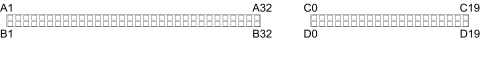
Connectors CN6 and CN7 carry the ISA bus signals. Figure 1 shows the PC/104 A and B pin layout for CN6, and the C and D pin layout for CN7.
| CN6 Connector Pinout | CN7 Connector Pinout | ||||||
| IOCHCHK- | A1 | B1 | GND | GND | D0 | D0 | GND |
| SD7 | A2 | B2 | RESETDRV | SBHE- | D1 | D1 | MEMCS16-- |
| SD6 | A3 | B3 | +5V | LA23 | D2 | D2 | IOCS16- |
| SD5 | A4 | B4 | IRQ9 | LA22 | D3 | D3 | IRQ10 |
| SD4 | A5 | B5 | -5V | LA21 | D4 | D4 | IRQ11 |
| SD3 | A6 | B6 | DRQ2 | LA20 | D5 | D5 | IRQ12 |
| SD2 | A7 | B7 | -12V | LA19 | D6 | D6 | IRQ15 |
| SD1 | A8 | B8 | ENDXFR- | LA18 | D7 | D7 | IRQ14 |
| SD0 | A9 | B9 | +12V | LA17 | D8 | D8 | DACK0- |
| IOCHRDY | A10 | B10 | keyed | MEMR- | D9 | D9 | DRQ0 |
| AEN | A11 | B11 | SMEMW- | MEMW- | D10 | D10 | DACK5- |
| SA19 | A12 | B12 | SMEMR- | SD8 | D11 | D11 | DRQ5 |
| SA18 | A13 | B13 | IOW- | SD9 | D12 | D12 | DACK6- |
| SA17 | A14 | B14 | IOR- | SD10 | D13 | D13 | DRQ6 |
| SA16 | A15 | B15 | DACK3- | SD11 | D14 | D14 | DACK7- |
| SA15 | A16 | B16 | DRQ3 | SD12 | D15 | D15 | DRQ7 |
| SA14 | A17 | B17 | DACK1- | SD13 | D16 | D16 | +5 |
| SA13 | A18 | B18 | DRQ1 | SD14 | D17 | D17 | MASTER- |
| SA12 | A19 | B19 | REFRESH- | SD15 | D18 | D18 | GND |
| SA11 | A20 | B20 | SYSCLK | keyed | D19 | D19 | GND |
| SA10 | A21 | B21 | IRQ7 | ||||
| SA9 | A22 | B22 | IRQ6 | ||||
| SA8 | A23 | B23 | IRQ5 | ||||
| SA7 | A24 | B24 | IRQ4 | ||||
| SA6 | A25 | B25 | IRQ3 | ||||
| SA5 | A26 | B26 | DACK2- | ||||
| SA4 | A27 | B27 | TC | ||||
| SA3 | A28 | B28 | BALE | ||||
| SA2 | A29 | B29 | +5V | ||||
| SA1 | A30 | B30 | OSC | ||||
| SA0 | A31 | B31 | GND | ||||
| GND | A32 | B32 | GND | ||||
The PC/104-Plus bus is essentially identical to the PCI Bus except for the physical design. A single pin and socket connector is specified for the bus signals. A 120-pin header, J3, arranged as four 30-pin rows incorporates a full 32-bit, 33MHz PCI Bus. The additional pins on the PC/104-Plus connectors are used as ground or key pins. The female sockets on the top of the board enable stacking another PC/104-Plus board on top of the Poseidon board.
| A | B | C | D | |
| 1 | GND/5.0V KEY | Reserved | +5V | AD00 |
| 2 | VI/O | AD02 | AD01 | +5V |
| 3 | AD05 | GND | AD04 | AD03 |
| 4 | C/BE0* | AD07 | GND | AD06 |
| 5 | GND | AD09 | AD08 | GND |
| 6 | AD11 | VI/O | AD10 | M66EN |
| 7 | AD14 | AD13 | GND | AD12 |
| 8 | +3.3V | C/BE1* | AD15 | +3.3V |
| 9 | SERR* | GND | Reserved | PAR |
| 10 | GND | PERR* | +3.3V | Reserved |
| 11 | STOP* | +3.3V | LOCK* | GND |
| 12 | +3.3V | TRDY* | GND | DESEL* |
| 13 | FRAME* | GND | IRDY* | +3.3V |
| 14 | GND | AD16 | +3.3V | C/BE2* |
| 15 | AD18 | +3.3V | AD17 | GND |
| 16 | AD21 | AD20 | GND | AD19 |
| 17 | +3.3V | AD23 | AD22 | +3.3V |
| 18 | IDSEL0 | GND | IDSEL1 | IDSEL2 |
| 19 | AD24 | C/BE3* | VI/O | IDSEL3 |
| 20 | GND | AD26 | AD25 | GND |
| 21 | AD29 | +5V | AD28 | AD27 |
| 22 | +5V | AD30 | GND | AD31 |
| 23 | REQ0* | GND | REQ1* | VI/O |
| 24 | GND | REQ2* | +5V | GNT0* |
| 25 | GNT1* | VI/O | GNT2* | GND |
| 26 | +5V | CLK0 | GND | CLK1 |
| 27 | CLK2 | +5V | CLK3 | GND |
| 28 | GND | INTD* | +5V | RST* |
| 29 | +12V | INTA* | INTB* | INTC* |
| 30 | -12V | REQ3* | GNT3* | GND/3.3V KEY |
On the Poseidon, all of the PCI circuitry is driven with 3.3V circuitry and is 5V tolerant. The main board can support either 3.3V or 5V-only cards. For this reason, the connector is not keyed (to prevent certain types of cards from being inserted).
Connector CN19 is a 2x4-pin header used to connect a mouse or keyboard.
| +5Vin | 1 | 2 | - |
| Keyboard data | 3 | 4 | Mouse data |
| Keyboard clock | 5 | 6 | Mouse clock |
| Ground | 7 | 8 | - |
| Signal | Definition |
| +5Vin | keyboard PS/2 pin 4 |
| Keyboard data | keyboard PS/2 pin 1 |
| Mouse data | mouse PS/2 pin 1 |
| Keyboard clock | keyboard PS/2 pin 5 |
| Mouse clock | mouse PS/2 pin 5 |
| Ground | PS/2 pin 3 |
Connector CN18 is a 2/4-pin header for access to the standard button/LED connections.
| Speaker | 1 | 2 | PW LED |
| ATX power button | 3 | 4 | - |
| Ground | 5 | 6 | Ground |
| Reset key | 7 | 8 | - |
The following table describes the CN18 connector pinouts.
| Signal | Definition |
| Speaker | The signal on the Speaker pin is referenced to +5V out. Connect a speaker between this pin and +5V out. |
| PW LED | Switched power output to connect a panel power LED. No series resistor needed. |
| ATX power button | The ATX power button should be tied to ground whenever the “Power Button” is used. The “Power Button” has different functionality, depending on the current system mode and software operation. In general, the following guidelines apply. NOTE: depending on the default configuration, the system usually powers-up immediately as power is applied. When ATX is enabled, a momentary contact between this pin and Ground causes the CPU to turn on and a contact of four seconds or longer generates a power shutdown. ATX power control is enabled using a jumper on jumper block JP7. |
| Ground | Ground |
| Reset key | Connection between Reset key and ground generate a reset condition. The board remains in a reset state (with non-standby power rails disabled) until Reset key is removed from ground. |
Poseidon includes a 2x17-pin header, CN12, for all digital data acquisition I/O.
| DIO A7 | 1 | 2 | DIO A6 |
| DIO A5 | 3 | 4 | DIO A4 |
| DIO A3 | 5 | 6 | DIO A2 |
| DIO A1 | 7 | 8 | DIO A0 |
| DIO B7 | 9 | 10 | DIO B6 |
| DIO B5 | 11 | 12 | DIO B4 |
| DIO B3 | 13 | 14 | DIO B2 |
| DIO B1 | 15 | 16 | DIO B0 |
| DIO C7 | 17 | 18 | DIO C6 |
| DIO C5 | 19 | 20 | DIO C4 |
| DIO C3 | 21 | 22 | DIO C2 |
| DIO C1 | 23 | 24 | DIO C0 |
| DIN0/CLK0 | 25 | 26 | DIN1/GATE0 |
| DOUT0/CTROUT0 | 27 | 28 | DOUT2/CTROUT2 |
| AD_RCB | 29 | 30 | DOUT1/SHOUT |
| DIN3/EXTCLK | 31 | 32 | DIN2/EXTGATE |
| +5V out | 33 | 34 | Ground |
| Signal | Definition |
| DIO A7-A0 | Digital I/O port A; programmable direction |
| DIO B7-B0 | Digital I/O port B; programmable direction |
| DIO C7-C0 | Digital I/O port C; programmable direction |
| DIN0-1 | Digital input port with counter/timer and external trigger functions |
| DOUT0-2 | Digital output port with counter/timer functions |
| CLK0 | Input source to Ctr 0 |
| GATE0 | Pin to control gating of Ctr 0 |
| CROUT0 | Counter 0 output |
| CROUT2 | Counter 2 output |
| AD_RCB | A/D convert signal output; can be used to synchronize multiple boards |
| SHOUT | - |
| EXTCLK | External A/D trigger input; Also used for digital interrupt (DINT) input |
| EXTGATE | Pin to control gating of Ctrs 1& 2 for A/D timing |
| +5V out | Connected to switched +5V supply (Output only! Do not connect to external supply) |
| Ground | Digital ground (0V - reference); used for digital circuitry only |
Connector CN13 is a 2x20-pin header used for analog I/O data acquisition.
| Single-ended | Differential | |||||||
| Vin 0 | 1 | 2 | Vin 16 | Vin 0 + | 1 | 2 | Vin 0 - | |
| Vin 1 | 3 | 4 | Vin 17 | Vin 1 + | 3 | 4 | Vin 1 - | |
| Vin 2 | 5 | 6 | Vin 18 | Vin 2 + | 5 | 6 | Vin 2 - | |
| Vin 3 | 7 | 8 | Vin 19 | Vin 3 + | 7 | 8 | Vin 3 - | |
| Vin 4 | 9 | 10 | Vin 20 | Vin 4 + | 9 | 10 | Vin 4 - | |
| Vin 5 | 11 | 12 | Vin 21 | Vin 5 + | 11 | 12 | Vin 5 - | |
| Vin 6 | 13 | 14 | Vin 22 | Vin 6 + | 13 | 14 | Vin 6 - | |
| Vin 7 | 15 | 16 | Vin 23 | Vin 7 + | 15 | 16 | Vin 7 - | |
| Vin 8 | 17 | 18 | Vin 24 | Vin 8 + | 17 | 18 | Vin 8 - | |
| Vin 9 | 19 | 20 | Vin 25 | Vin 9 + | 19 | 20 | Vin 9 - | |
| Vin 10 | 21 | 22 | Vin 26 | Vin 10 + | 21 | 22 | Vin 10 - | |
| Vin 11 | 23 | 24 | Vin 27 | Vin 11 + | 23 | 24 | Vin 11 - | |
| Vin 12 | 25 | 26 | Vin 28 | Vin 12 + | 25 | 26 | Vin 12 - | |
| Vin 13 | 27 | 28 | Vin 29 | Vin 13 + | 27 | 28 | Vin 13 - | |
| Vin 14 | 29 | 30 | Vin 30 | Vin 14 + | 29 | 30 | Vin 14 - | |
| Vin 15 | 31 | 32 | Vin 31 | Vin 15 + | 31 | 32 | Vin 15 - | |
| Output ground | 33 | 34 | Vout 0 | Output ground | 33 | 34 | Vout 0 | |
| Vout 1 | 35 | 36 | Vout 2 | Vout 1 | 35 | 36 | Vout 2 | |
| Vout 3 | 37 | 38 | Analog ground | Vout 3 | 37 | 38 | Analog ground | |
| DIN3/EXTCLK | 39 | 40 | Digital ground | DIN3/EXTCLK | 39 | 40 | Digital ground | |
| Signal | Definition |
| Vout3-0 | Analog output channels 3 – 0 |
| Analog Ground | 0V analog reference |
| Vin 31 ~ Vin 0 | Analog input channels 31 – 0 in single-ended mode |
| Vin 15 + ~ Vin 0 + | High side of input channels 15 – 0 in differential mode |
| Vin 15 - ~ Vin 0 - | Low side of input channels 15 – 0 in differential mode |
| Digital ground | 0V digital reference |
| DIN3 | Digital input port with counter/timer and external trigger functions |
| EXTCLK | External A/D trigger input; Also used for digital interrupt (DINT) input |
NOTE: The reference grounds are NOT decoupled from the power grounds – they are indirectly connected to the power supply input (and other on-board ground/0V references). Do not assume that these grounds are floating. Do not apply a high-voltage input (relative to the power input ground) to these ground signals or to any other board I/O pin.
10/100/1000 BaseT (Gigabit) Ethernet connectivity is provided by connectors CN17. Connector CN17 is a 2x5-pin header.
| Common | 1 | 2 | - |
| DA+ | 3 | 4 | DA- |
| DB+ | 5 | 6 | DB- |
| DC+ | 7 | 8 | DC- |
| DD+ | 9 | 10 | DD- |
| Signal | Definition |
| DA+/- | Data A; bi-directional pair A+/A- |
| DB+/- | Data B; bi-directional pair B+/B- |
| DC+/- | Data C; bi-directional pair C+/C- |
| DD+/- | Data D; bi-directional pair D+/D- |
Connector CN15 is a 2x5-pin header that provides audio connectivity.
| Left headphone/Line out | 1 | 2 | Right headphone/Line out |
| Audio ground | 3 | 4 | Left line input |
| Right line input | 5 | 6 | Audio ground |
| Microphone input | 7 | 8 | Power reference |
| - | 9 | 10 | Audio ground |
| Signal | Definition |
| Headphone/Line Out | Line Level output, capable of driving headphones, which is referred to as “Headphone Out” in most sound documentation. |
| Line Input | Line-Level input, which is referred to as “Line In” in most sound documentation. |
| Microphone Input | Microphone-level mono input; phantom power provided via pin 9. |
| Power reference | Microphone power reference |
| Audio ground | Ground |
The Poseidon sound chip is AC97-compatible. The “Line Out” is powered and used for the amplified Speaker Connector output, J13, described below. The line-level output listed above is listed as either “Headphone Out” or “Line Out 2” in most of the software and documentation for this sound interface.
Connector CN11 is a 2x4-pin header used to connect speakers.
| Speaker left high (+) | 1 | 2 | Speaker left low (-) |
| Speaker right high (+) | 3 | 4 | Speaker right low (-) |
| Volume, high | 5 | 6 | Volume, mid |
| Volume, low | 7 | 8 | - |
| Signal | Definition |
| Speaker LEFT +/- | Speaker Connection Pair for LEFT speaker (4-Ohm Speaker) |
| Speaker RIGHT +/- | Speaker Connection Pair for RIGHT speaker (4-Ohm Speaker) |
| Mono Output | Line-Level mono output (for reference) |
| Volume – LOW, MID, HIGH | These are volume controls for the attached speakers |
The volume control is capable of 32 discrete levels, ranging from a 20dB maximum gain to -85dB (Muted). The main volume control is the “MID” line, which may be tied to the center tap of a potentiometer with “HIGH” on one side and “LOW” on the other to give a full range of power control.
The maximum output power is specified to provide up to two Watts into a 4-Ohm speaker load. Note that this output power is drawn from the on-board 5V supply.
The speakers are driven using a Bridged-Tied Load (BTL) amplifier configuration. This is a differential speaker connection. As such, each speaker should be wired directly to the appropriate pair of connections for that speaker.
Connector CN10 provides switched power for use with external drives. If ATX is enabled, the power is switched ON and OFF with the ATX input switch. If ATX is not enabled, the power is switched ON and OFF in conjunction with the external power.

| 1 | +5v (switched) |
| 2 | Ground |
| 3 | Ground |
| 4 | +12v (switched) |
| Signal | Definition |
| +5v | This is provided by the on-board power supply, derived from the input power. It is switched off when the board is powered down. |
| +12v | This is provided by the 12V input pin on the main power connector. It is switched off when the board is powered down. |
| Ground | These are 0V ground references for the power output voltage rails, above. |
Diamond Systems Corporation cable no. 698006 mates with J15. This cable provides a standard full-size power connector for a hard drive or CD-ROM drive and a standard miniature power connector for a floppy drive.
Connector CN2 is a 2x22-pin header used for the IDE connection.
| Reset - | 1 | 2 | Ground |
| D7 | 3 | 4 | D8 |
| D6 | 5 | 6 | D9 |
| D5 | 7 | 8 | D10 |
| D4 | 9 | 10 | D11 |
| D3 | 11 | 12 | D12 |
| D2 | 13 | 14 | D13 |
| D1 | 15 | 16 | D14 |
| D0 | 17 | 18 | D15 |
| Ground | 19 | 20 | Key (not used) |
| DRQ | 21 | 22 | Ground |
| IDEIOW- | 23 | 24 | Ground |
| IDEIOR- | 25 | 26 | Ground |
| IORDY | 27 | 28 | Ground |
| DACK- | 29 | 30 | Ground |
| IRQ15 | 31 | 32 | Pulled low for 16-bit operation |
| A1 | 33 | 34 | Not used |
| A0 | 35 | 36 | A2 |
| CS1- | 37 | 38 | CS3- |
| LED- | 39 | 40 | Ground |
| +5v | 41 | 42 | +5v |
| Ground | 43 | 44 | Not used |
Connector CN20 is a 2x20-pin header that provides access to the four on-board serial ports. The PORT1 and PORT2 serial ports are always configured for RS-232. The PORT3 and PORT4 serial ports are independently, software configurable as either RS-232, RS-485 or RS-422. All four serial ports are independently enabled.
| Port No. | Pin Assignment |
| PORT1 | Pins 1 - 10 |
| PORT2 | Pins 11 - 20 |
| PORT3 | Pins 21 - 30 |
| PORT4 | Pins 31 - 40 |
The following tables list the signals for each mode of operation, including the DE-9 pin numbers associated with the signals.
| COM1: DCD1 | 1 | 2 | DSR1 |
| RXD1 | 3 | 4 | RTS1 |
| TXD1 | 5 | 6 | CTS1 |
| DTR1 | 7 | 8 | RI1 |
| GND | 9 | 10 | N/C |
| COM2: DCD2 | 11 | 12 | DSR2 |
| RXD2 | 13 | 14 | RTS2 |
| TXD2 | 15 | 16 | CTS2 |
| DTR2 | 17 | 18 | RI2 |
| GND | 19 | 20 | - |
| COM3: DCD3 | 21 | 22 | DSR3 |
| RXD3 | 23 | 24 | RTS3 |
| TXD3 | 25 | 26 | CTS3 |
| DTR3 | 27 | 28 | RI3 |
| GND | 29 | 30 | N/C |
| COM4: DCD4 | 31 | 32 | DSR4 |
| RXD4 | 33 | 34 | RTS4 |
| TXD4 | 35 | 36 | CTS4 |
| DTR4 | 37 | 38 | RI4 |
| GND | 39 | 40 | - |
| Signal | Definition | DE-9 Pin | Direction |
| DCDn | Data Carrier Detect | pin 1 | Input |
| DSRn | Data Set Ready | pin 6 | Input |
| RXDn | Receive Data | pin 2 | Input |
| RTSn | Request to Send | pin 7 | Output |
| TXDn | Transmit Data | pin 3 | Output |
| CTSn | Clear to Send | pin 8 | Input |
| DTRn | Data Terminal Ready | pin 4 | Output |
| RIn | Ring Indicator | pin 9 | Input |
| GND | Ground | - | - |
Only CN20 connector pins 21 through 40, PORT3 and PORT4, are used for RS-485.
| COM3: NC | 21 | 22 | NC |
| TXD/RXD+3 | 23 | 24 | TXD/RXD-3 |
| GND | 25 | 26 | NC |
| NC | 27 | 28 | NC |
| GND | 29 | 30 | NC |
| COM4: NC | 31 | 32 | NC |
| TXD/RXD+4 | 33 | 34 | TXD/RXD-4 |
| GND | 35 | 36 | NC |
| NC | 37 | 38 | NC |
| GND | 39 | 40 | NC |
| Signal | Definition | DE-9 Pin | Direction |
| TXD/RXD+n | Differential Transceiver Data (HIGH) | pin 2 | bi-directional |
| TXD/RXD-n | Differential Transceiver Data (LOW) | pin 7 | bi-directional |
| GND | Ground | - | - |
| NC | (not connected) | - | - |
Only CN20 connector pins 21 through 40, PORT3 and PORT4, are used for RS-422.
| COM3: NC | 21 | 22 | NC |
| TXD+1 | 23 | 24 | TXD-1 |
| GND | 25 | 26 | RXD-1 |
| RXD+1 | 27 | 28 | NC |
| GND | 29 | 30 | NC |
| COM4: NC | 31 | 32 | NC |
| TXD+2 | 33 | 34 | TXD-2 |
| GND | 35 | 36 | RXD-2 |
| RXD+2 | 37 | 38 | NC |
| GND | 39 | 40 | NC |
| Signal | Definition | DE-9 Pin | Direction |
| TXD+n/TXD-n | Differential transmit data | - | Output |
| RXD+n/RXD-n | Differential receive data | - | Input |
| GND | Ground | - | - |
| NC | (not connected) | - | - |
Connector CN8 is used to connect an external battery. The battery voltage for this input should be 3-3.5V. The current draw averages under 4µA at 3V.

| 1 | Battery input (+) |
| 2 | Ground |
In addition to the external battery connected to CN8, the on-board battery and an additional external battery input on Utility Connector CN18 are other possible sources for maintaining the Real-Time Clock and the CMOS settings (BIOS settings for various system configurations). The battery that has the highest voltage will see the majority of the current draw, which is minimal. Note that there must be a battery voltage input for the default power-up mode.
Connector CN1 provides access to the internal LVDS LCD display drivers. Note that the LCD also requires the backlight to be connected (CN4, below) to function correctly.

| LCD1 data 0- | 1 | 2 | LCD2 data 0- |
| LCD1 data 0+ | 3 | 4 | LCD2 data 0+ |
| Ground | 5 | 6 | Ground |
| LCD1 data 1- | 7 | 8 | LCD2 data 1- |
| LCD1 data 1+ | 9 | 10 | LCD2 data 1+ |
| Ground | 11 | 12 | Ground |
| LCD1 data 2- | 13 | 14 | LCD2 data 2- |
| LCD1 data 2+ | 15 | 16 | LCD2 data 2+ |
| Ground | 17 | 18 | Ground |
| LCD1 clock- | 19 | 20 | LCD2 clock- |
| LCD1 clock+ | 21 | 22 | LCD2 clock+ |
| Ground | 23 | 24 | Ground |
| LCD1 data 3- | 25 | 26 | LCD2 data 3- |
| LCD1 data 3+ | 27 | 28 | LCD2 data 3+ |
| VDD (LCD display) | 29 | 30 | VDD (LCD display) |
| Signal | Definition |
| LCD1 Data 3-0 +/- | Primary Data Channel, bits 3-0 (LVDS Differential signaling) |
| LCD1 Clock +/- | Primary Data Channel, Clock (LVDS Differential signaling) |
| LCD2 Data 3-0 +/- | Secondary Data Channel, bits 3-0 (LVDS Differential signaling) |
| LCD2 Clock +/- | Secondary Data Channel, Clock (LVDS Differential signaling) |
| VDD | +3.3V Switched Power Supply for LCD display (only powered up when LCD display is active) |
| Ground | Power Ground, 0V |
Connector CN16 is a 2x5-pin header for connecting a VGA monitor.
| Red | 1 | 2 | Ground |
| Green | 3 | 4 | - |
| Blue | 5 | 6 | Ground |
| HSYNC | 7 | 8 | DDC data |
| VSYNC | 9 | 10 | DDC clock |
| Signal | Definition |
| Red | RED signal (positive, 0.7Vpp into 75 Ohm load) |
| R-Ground | Ground return for RED signal |
| Green | GREEN signal (positive, 0.7Vpp into 75 Ohm load) |
| G-Ground | Ground return for GREEN signal |
| Blue | BLUE signal (positive, 0.7Vpp into 75 Ohm load) |
| B-Ground | Ground return for BLUE signal |
| DDCclock/data | Digital serial I/O signals used for monitor detection (DDC1 specification) |
| HSYNC | Horizontal sync |
| VSYNC | Vertical sync |
Note: While the DDC serial detection pins are present, a 5V power supply is not provided (the old “Monitor ID” pins are also not used).
Connector CN4 provides the backlight power and control for the optional LCD panel. See the description for connector CN1, above, for details on the LCD data interface.

| 1 | +12v |
| 2 | Control |
| 3 | Ground |
| Signal | Definition |
| Control | Output signal (from Poseidon) to allow power-down of backlight |
| +12V | Power supply for LCD Backlight assembly |
| Ground | Ground for LCD Backlight assembly |
The control signal is used to allow the system to power-down the backlight when the system enables monitor-power-down during power management control.
The +12V supply is removed when the system is powered down.
The standard Poseidon input power is supplied through the CN9 connector from an external mid-range supply.

| PS_ON | 1 | 5 | +5V standby |
| Ground | 2 | 6 | +5V in |
| Ground | 3 | 7 | +5V in |
| +12V in | 4 | 8 | Ground |
| Signal | Definition |
| +5V in | +5V main input power. |
| Ground | 0-V (ground) power return path. |
| +12V in | Power supply for in-board 12V devices, including hard drives, auxiliary power, PC/104 power, and LCD backlight. Range should be 11.9V to 13.5V measured at this connector. |
| +5V standby | +5V standby power; powers board when in standby mode. |
| PS_ON | Power Supply ON. Feedback pin for external ATX supply, when needed; pulled low when on-board power is inactive. |
Poseidon in the standard, mid-range power input configuration supports a voltage range from +4.75V to +5.25V, with some restrictions.
The “+12V” power supply input is intended for all on-board and board-controlled 12V power supplies, including the PC/104-Plus 12V supplies, the external hard drive power supply (through connector J15, described above), and the LCD backlight. If these devices are not used, the “+12V” input may be left unconnected.
Make certain that your power supply has enough current capacity to drive your system. The Poseidon requires 12 to 20 Watts or more, depending on which external devices are connected to the board. This could require over 4A on the “+Vin” line at minimum voltage inputs. In particular, many disk drives need extra current during startup. If your system fails to boot properly or if disk accesses do not work correctly, the first thing to check is the power supply voltage level. Many boot-up problems are caused simply by insufficient voltage due to excess current draw on the “+Vin” supply during initialization.
Multiple +5V and ground pins are provided for extra current carrying capacity, if needed. Each pin is rated at 3A max (15W). For the Poseidon CPU with a moderate I/O device complement (basic hard drive, key board, mouse, USB devices, and a network PC/104-Plus card, for example).
ATX control enables the +5V and +12V power to be switched ON and OFF with an external momentary switch. A short press on the switch turns ON power, and holding the switch on for four seconds or longer turns OFF power (See the Utility Header description for connector CN18, above).
Connector CN21 is a 2x10 pin headers for connecting USB 0/1 and USB 2/3, each providing USB 2.0 480Mbps maximum transfer rates.
| - | 1 | 2 | Shield |
| Shield | 3 | 4 | Shield |
| USB3 data+ | 5 | 6 | USB2 data+ |
| USB3 data- | 7 | 8 | USB2 data- |
| USB2/3 power | 9 | 10 | USB2/3 power |
| - | 11 | 12 | Shield |
| Shield | 13 | 14 | Shield |
| USB1 data+ | 15 | 16 | USB0 data+ |
| USB1 data- | 17 | 18 | USB0 data- |
| USB0/1 power | 19 | 20 | USB0/1 power |
| Signal | Definition |
| Shield | ground |
| USB0-3 power- | +5V power for USB ports 0-3 |
| USB0-3 data+ | data + for USB ports 0-3 |
| USB0-3 data- | data - for USB ports 0-3 |
Connector CN5 is the serial ATA connector.

| 1 | Ground |
| 2 | TX+ |
| 3 | TX- |
| 4 | Ground |
| 5 | RX- |
| 6 | RX+ |
| 7 | Ground |
| 8 | Ground |
| 9 | Ground |
| Signal | Definition |
| TX+/TX- | Differential outputs to PHY |
| RX+/RX- | Differential inputs from PHY |
| Ground | Ground |
Connector CN14 is a 2x10-pin header providing I/O panel power.
| +5V in | 1 | 2 | +5V in |
| +5V in | 3 | 4 | +5V in |
| +5V in | 5 | 6 | +5V in |
| +5V in | 7 | 8 | +5V in |
| Ground | 9 | 10 | Ground |
| Ground | 11 | 12 | Ground |
| Ground | 13 | 14 | Ground |
| Ground | 15 | 16 | Ground |
| +12V in | 17 | 18 | +12V in |
| +5V standby | 19 | 20 | PS_ON |
| Signal | Definition |
| +5V in | +5V input |
| +12V in | +12V input |
| +5V standby | +5V standby power; powers board when in standby mode. |
| PS_ON | Power Supply ON. Feedback pin for external ATX supply, when needed; pulled low when on-board power is inactive. |
| Ground | Ground |
Note: Optionally, a PC/104 power supply may be used to power the board through the PC/104 bus.
Connector J1 is the JTAG configuration interface for factory use and firmware upgrade.
| 1 | +3.3V |
| 2 | GND |
| 3 | CTCK |
| 4 | FTDO |
| 5 | CTDI |
| 6 | CTMS |
| Signal | Definition |
| +3.3V | Power |
| GND | Ground |
| CTCK | Test clock input |
| FTDO | Test data output |
| CTDI | Test data input |
| CTMS | Test mode select |
Connector J2 is the reference voltage test point for use during factory calibration.
| 1 | +Vref |
| 2 | GND |
| Signal | Definition |
| +Vref | Reference voltage |
| GND | Ground |