
The Poseidon board has the following jumper-selectable configuration options.
| Jumper Block | Configuration Functions |
| JP1 | PCI VI/O voltage setting |
| JP2 | DAQ configuration:DMA level |
| JP3 | COM3/COM4/ADC IRQ configuration |
| JP4 | Analog I/O single-ended/differential configuration |
| JP5 | DAC configuration |
| JP6 | Battery connection (CMOS RAM erase) |
| JP7 | ATX power |
| JP8 | RS-422/RS-485 termination |
| JP9 | DIO pull-up/pull-down |
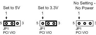
JP1 provides simple access to the VIO setting for PC/104-Plus cards. This setting sets the voltage supplied on the “VIO” power pins of the PC/104-Plus connector (J3). Note that the “VIO” voltage is used on most cards to supply the I/O Voltage for all PCI signals.
| JP1 | |
| Pin Label | Function |
| 3 | Main +3.3v power supply on boardconnect pins 3-PCI VIO to select +3.3v |
| PCI VIO | PCI VIO for selecting either +3.3v or +5v onboard power supply. |
| 5 | Main +5v power supply on boardconnect pins 5-PCI VIO to select +5v |
The Poseidon can support either I/O voltage range (all on-board signals are driven from 3.3V power rails, but are 5V tolerant), so the determination of the I/O voltage is entirely dependent on the types of PC/104-Plus cards plugged into the system.
PC/104-Plus cards should be keyed to identify the correct voltage setting. No key means that the card is universal and can accept either power setting. There are essentially 4 possibilities:
The first three possibilities can be easily determined by checking the keying of the card, as shown in the following table.
| Card Voltage Type | Pin Configuration |
| 5V card | Pin A1 missing/pin D30 present |
| 3.3V card | Pin A1 present/pin D30 missing |
| Universal card | Pin A1 present/pin D30 present |
The only solution for cards that are incorrectly keyed is to read the documentation and verify the I/O voltage (if it is called out in the card description). While not a widespread issue, this is something to be aware of when starting to work with a new PC/104-Plus card.
Note that this voltage selection is not used for standard PC/104 cards; only the PCI-signaling of PC/104-Plus.
Figure 12 shows how to select the desired voltage using jumper JP1.
Jumper block JP2 is used for base address selection, to select DMA level and to select 16- or 8-bit data bus operation.
Each board in a PC/104 system must have its own unique block of addresses that does not overlap with any other board in the system or feature on the CPU. The lowest address of this address block is called the base address. The Poseidon base address is set using JP2 pins 9-14, as shown below. The table lists the possible jumper configurations, using pins 9-14, and corresponding base addresses.
| Base Address | 9-10 | 11-12 | 13-14 |
| 140h | In | In | In |
| 340h | In | In | Out |
| 100h | In | Out | In |
| 180h | In | Out | Out |
| 200h | Out | In | In |
| 280h | Out | In | Out |
| 300h (default) | Out | Out | In |
| 380h | Out | Out | Out |
For example, Figure 3 shows the pin configuration for base address 100h.
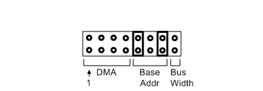
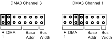
Jumper block JP2 contains pins for selecting the DMA level. Select either DMA channel 1 or DMA channel 3, as shown in Figure 4, below. Both pin pairs must be connected to select the desired channel.
The default configuration is no DMA and 8-bit bus width.
Note: DMA is supported in the hardware, however it is not currently supported in Diamond Systems’ Universal Driver software.
On boards without FIFOs or memory buffers, DMA is required to support high-speed sampling at rates above the maximum sustainable interrupt rate, which may vary from 1,000 to 20,000 depending on the CPU and operating system. However, Poseidon contains a 1024-sample FIFO for A/D data that allows the interrupt rate to be much slower than the sample rate. The board can support full-speed sampling at up to 250,000 samples per second without the use of DMA.
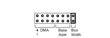
The board can be configured for 16-bit read operations when reading the A/D data. To do this, jumper pins 15 and 16 on JP2. A 16-bit transfer only occurs during a 16-bit read instruction from the base address, A/D data, when the jumper is installed. Otherwise, the A/D board and host CPU ignore the 16-bit setting and/or instruction and convert the 16-bit operation into two 8-bit read operations.
Jumper pins 15 and 16, as shown in Figure 5, below, to select 16-bit operation.
Jumper block JP3 is used to configure IRQ levels for COM3, COM4 and ADC.
| JP3 | |
| Pin | Function |
| 1 | IRQ10; selectable for COM3 and COM4 |
| 2 | COM3 IRQ select |
| 3 | COM4 IRQ select |
| 4 | IRQ7; selectable for COM3 and COM4 |
| 5 | IRQ3; selectable for COM3 and COM4 |
| 6 | COM3 IRQ select |
| 7 | COM3 IRQ select |
| 8 | IRQ4; selectable for COM3 |
| 9 | IRQ5; selectable for AD and COM3 |
| 10 | IRQ AD select |
| 11 | COM3 IRQ select |
| 12 | IRQ6; selectable for AD and COM3 |
Note: Boards Rev A1 have a different configuration table that can be found in Appendix A.
The default configuration is IRQ7 for COM3, IRQ10 for COM4 and IRQ5 for A/D.
The example in Figure 6 show the jumper settings for configuring COM4 for IRQ3, COM3 for IRQ6 and ADC for IRQ5.

The input channels on Poseidon can be configured as 32 single-ended, 16 differential, or 16 single-ended plus 8 differential. Four different configurations are possible for the Data Acquisition (Analog I/O) connector, CN13.
A single-ended input is a single-wire input, plus ground, that is measured with reference to the board’s analog ground. For accurate measurement, the board’s ground must be at the same potential as the source signal’s ground. Usually this is accomplished by connecting the two grounds together at some point.
A differential input is a two-wire input, plus ground, that is measured by subtracting the low input from the high input. This type of connection offers two advantages.
It allows for greater noise immunity, because the noise, which is present in equal amounts and equal phase on both the high and low inputs, is subtracted out when the low input is subtracted from the high input.
It allows for the signal to float away from ground. Normally the ground of the signal source is still connected to the ground on the A/D board in order to keep the signal from straying out of the common mode range of the A/D board’s input circuitry.
To configure the input channels, set the pin pairs in jumper block JP4 according to the table, below.
Note: For safety reasons, do not modify JP4 while the board is powered on.
| Connector Pin Configuration | 1-2 | 3-4 | 5-6 | 7-8 | 9-10 | 11-12 |
| Inputs 0-31, single-ended (default) | In | In | Out | Out | Out | Out |
| Inputs 0-15, differential | Out | Out | In | In | In | In |
| Inputs 0-7, differential Inputs 8-15, single-ended Inputs 24-31, single-ended |
Out | In | In | Out | In | Out |
| Inputs 0-7, single-ended Inputs 8-15, differential Inputs 16-23, single-ended |
In | Out | Out | In | Out | In |
For example, Figure 7 shows the JP4 jumper settings to configure CN13 pins 0-15 for differential mode.

The analog outputs on Poseidon can be set to operate in bipolar (both + and –) or unipolar (+ only) output voltage ranges. In addition, the full-scale output range can be set to 5V, 10V, or programmable. The maximum output current on any channel is 5mA. Current outputs such as 0-20mA outputs are not supported.
On power-up, the DACs can be configured to reset to mid-scale (0V in bipolar mode) or zero scale (0V in unipolar mode). Generally, the reset mode should be selected so that the DACs power-up to 0V.
In programmable mode, the full-scale output voltage can be set anywhere from 0V to 10V in software. You must use the Universal Driver software to set programmable D/A range, because it requires calibration to fine-tune the setting to the desired value.
To configure the analog output range, set jumper block JP5 according to the tables below. The first four positions are used for the output range, and the fifth position is for the power-up reset mode.
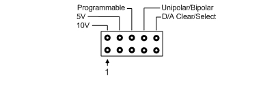
| Output Range | 10V | 5V | Programmable | Polarity | D/A Clear/Select |
| ±5V | Out | In | Out | In | X |
| ±10V | In | Out | Out | In | X |
| 0-5V | Out | In | Out | Out | X |
| 0-10V | In | Out | Out | Out | X |
| Programmable, unipolar | Out | Out | In | Out | X |
| Programmable, bipolar | Out | Out | In | In | X |
Note: Programmable mode requires use of driver software to set and calibrate range.
The default configuration is 5V, unipolar.
Figure 9 shows the JP5 configuration for setting the output range to ±5V.

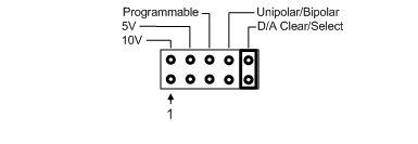
The following table shows the jumper position for power-up reset mode.
| Output Range | 10V | 5V | Programmable | Polarity | D/A Clear/Select |
| Mid-scale, bipolar modes | X | X | X | X | Out |
| Zero scale, unipolar modes | X | X | X | X | In |
Figure 10 shows the jumper setting to configure the DACs to reset to zero scale. (Omit the jumper to reset to mid-scale).
The CMOS RAM may be cleared using the 3-pin JP6 jumper block. By default, there are jumpers on pins one and two for standard BIOS configuration.

With the jumper in position 1-2, the CPU powers up with the default BIOS settings. Follow these steps to clear the CMOS RAM.
Note: Before erasing CMOS RAM, write down any custom BIOS settings.
The ATX power control is set using the JP7 ATX jumper block. ATX power control has the following behavior.
If the ATX jumper is removed, the battery-backup for CMOS and the real-time clock settings do not function when power is removed.
Figure 12 shows the ATX configuration options using the JP7 jumper block. (Pin 3 is not connected).
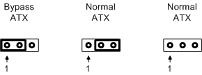
The default configuration is ATX bypass.
If the Poseidon board is the last card in a RS-422/RS-485 link, the link must be terminated. Use jumper block JP9 to terminate RS-422 and RS-485 lines for COM3 and COM4. Figure 13 shows the termination configuration options.
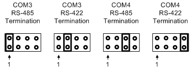
The default configuration is no termination.
Configure the DIO lines for pull-up or pull-down using jumper block JP8, as shown in Figure 14.
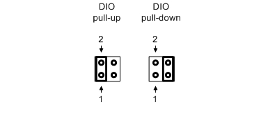
By default, the lines will not be pulled high or low.