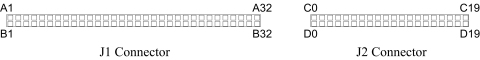
Figure 1: J1 and J2 Connectors
This section describes the connectors on the JANUS-MM board.
Connectors J1 and J2 carry the ISA bus signals. Figure 1 shows the PC/104 A and B pin layout for J1, and the C and D pin layout for J2.
Figure 1: J1 and J2 Connectors
| J1 Connector Pinout | J2 Connector Pinout | ||||||
| IOCHCHK- | A1 | B1 | GND | GND | D0 | D0 | GND |
| SD7 | A2 | B2 | RESETDRV | SBHE- | D1 | D1 | MEMCS16-- |
| SD6 | A3 | B3 | +5V | LA23 | D2 | D2 | IOCS16- |
| SD5 | A4 | B4 | IRQ9 | LA22 | D3 | D3 | IRQ10 |
| SD4 | A5 | B5 | -5V | LA21 | D4 | D4 | IRQ11 |
| SD3 | A6 | B6 | DRQ2 | LA20 | D5 | D5 | IRQ12 |
| SD2 | A7 | B7 | -12V | LA19 | D6 | D6 | IRQ15 |
| SD1 | A8 | B8 | ENDXFR- | LA18 | D7 | D7 | IRQ14 |
| SD0 | A9 | B9 | +12V | LA17 | D8 | D8 | DACK0- |
| IOCHRDY | A10 | B10 | keyed | MEMR- | D9 | D9 | DRQ0 |
| AEN | A11 | B11 | SMEMW- | MEMW- | D10 | D10 | DACK5- |
| SA19 | A12 | B12 | SMEMR- | SD8 | D11 | D11 | DRQ5 |
| SA18 | A13 | B13 | IOW- | SD9 | D12 | D12 | DACK6- |
| SA17 | A14 | B14 | IOR- | SD10 | D13 | D13 | DRQ6 |
| SA16 | A15 | B15 | DACK3- | SD11 | D14 | D14 | DACK7- |
| SA5 | A16 | B16 | DRQ3 | SD12 | D15 | D15 | DRQ7 |
| SA14 | A17 | B17 | DACK1- | SD13 | D16 | D16 | +5 |
| SA13 | A18 | B18 | DRQ1 | SD14 | D17 | D17 | MASTER- |
| SA12 | A19 | B19 | REFRESH- | SD15 | D18 | D18 | GND |
| SA11 | A20 | B20 | SYSCLK | keyed | D19 | D19 | GND |
| SA10 | A21 | B21 | IRQ7 | ||||
| SA9 | A22 | B22 | IRQ6 | ||||
| SA8 | A23 | B23 | IRQ5 | ||||
| SA7 | A24 | B24 | IRQ4 | ||||
| SA6 | A25 | B25 | IRQ3 | ||||
| SA5 | A26 | B26 | DACK2- | ||||
| SA4 | A27 | B27 | TC | ||||
| SA3 | A28 | B28 | BALE | ||||
| SA2 | A29 | B29 | +5V | ||||
| SA1 | A30 | B30 | OSC | ||||
| SA0 | A31 | B31 | GND | ||||
| GND | A32 | B32 | GND | ||||
The CAN bus interface supports CAN Specification 2.0, implementing the full CAN bus protocol.
JANUS-MM provides connectors for the two CAN ports. These are 10-pin right-angle, shrouded connectors (J7, J8) for CAN ports A and B. Optionally, non-standard 5-pin connectors (J14 and J15, located under the shroud) are provided for custom applications.
Use jumper J10 to select either the internal or external CAN A power options on the J7 (J14) connector. Use jumper J11 to select either the internal or external CAN B power options on the J8 (J15) connector. (Refer to section of this document).
NOTE: Connectors J7/J8 are depicted viewing the connector from the top edge of the board looking down.
 Figure 2: J7 Connector
| - | 1 | 2 | GNDA_CAN |
| CANLA | 3 | 4 | CANHA |
| GNDA_ISO | 5 | 6 | - |
| - | 7 | 8 | +5VA_CAN |
| - | 9 | 10 | - |
Figure 3: J8 Connector
| - | 1 | 2 | GNDB_CAN |
| CANLB | 3 | 4 | CANHB |
| GNDB_ISO | 5 | 6 | - |
| - | 7 | 8 | +5VB_CAN |
| - | 9 | 10 | - |
 Figure 4: J14 Connector
| 1 | GNDA_ISO |
| 2 | CANHA |
| 3 | CANLA |
| 4 | GNDA_CAN |
| 5 | +5VA_CAN |
Figure 5: J15 Connector
| 1 | GNDB_ISO |
| 2 | CANHB |
| 3 | CANLB |
| 4 | GNDB_CAN |
| 5 | +5VB_CAN |
Connector J13 is provided for connecting to any third-party TTL serial device. The signals for this connector are also used for the SocketModemTM. Therefore, this connector cannot be used if the SocketModemTM is installed.
Note: The modem signals are TTL level signals.
 Figure 6: J13 Connector
| 1 | DTR_MDM |
| 2 | DCD_MDM |
| 3 | CTS_MDM |
| 4 | DSR_MDM |
| 5 | RI_MDM |
| 6 | TXD_MDM |
| 7 | RXD_MDM |
| 8 | RTS_MDM |
| 9 | +5V |
| 10 | GND |
Connector J24 provides for connecting the Trimble Navigation GPS receiver card. Both the Lassen SKIITM and Lassen iQTM cards are supported. Refer to the vendor documentation for additional information on the hardware and software interface to the GPS. (See the Additional Information Section.)
Connector J12 provides two pins for GPS backup power and the pulse-per-second (PPS) signal, and two ground signals are also available.
 Figure 7: J12 Connector
| 1 | GND |
| 2 | GPS_BKUPPWR |
| 3 | GPS_PPS |
| 4 | GND |
Connector J24 provides for connecting the Trimble Navigation GPS receiver card. Both the Lassen SKIITM card and the Diamond Systems card using the Lassen iQTM module are supported. Refer to the vendor documentation for on the hardware and software interface to the GPS.
| 1 | TXD Port2 |
| 2 | Vcc |
| 3 | TXD Port1 |
| 4 | Backup Power |
| 5 | RXD Port1 |
| 6 | PPS |
| 7 | RXD Port2 |
| 8 | GND |
Connectors J20, J21, J22 and J23 provide for connecting the MultiTech SocketModemTM CDMA or SocketModemTM GPRS card. Refer to the vendor documentation in the Additional Information Section for the hardware and software interface to the wireless modem.
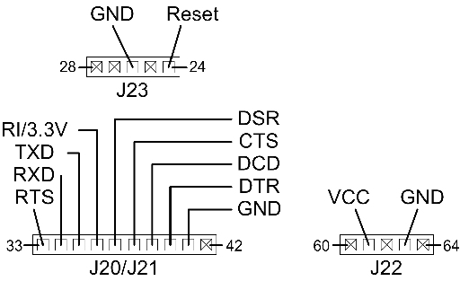 Figure 8: SmartModemTM Connector Signals
| 33 | RTS |
| 34 | RXD |
| 35 | TXD |
| 36 | RI/3.3V |
| 37 | DSR |
| 38 | CTS |
| 39 | DCD |
| 40 | DTR |
| 41 | GND |
| 42 | keyed |
| 60 | keyed |
| 61 | VCC |
| 62 | keyed |
| 63 | GND |
| 64 | keyed |
| 24 | Reset |
| 25 | keyed |
| 26 | GND |
| 27 | keyed |
| 28 | keyed |